|
|
|
|
|
|
|
|
|
|
|
|
MITite: designing materials from first principles
A novel class of semiconductors is introduced, based on computational design, to solve the long-standing problem of lattice and polarity mismatch in heteroepitaxial growth of III-V alloys on silicon substrates. (Phys. Rev. Lett. 82, pp. 3304, (1999))
Ab initio total-energy calculations and quasi-particle GW calculations are used to investigate the physical properties of these new semiconductors. One particular configuration is designed to match lattice constant and polarity with the Si(100) surface and to possess a direct band gap of 1.59 µm, which is close to the canonical frequency used by the optoelectronics industry. These results could pave the way for eventual monolithic integration of optical materials on silicon.
Background
In the optoelectronics industry, the canonical wavelength is 1.55 µm because of the efficiency of transmitting signals through fiberoptic cables at this wavelength. In order to design an optically-active (i.e. direct-gap) semiconductor near 1.55 µm, the industry has explored a large number of possible III-V alloys and II-VI alloys.
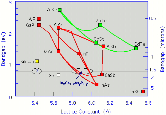
In the figure above, we illustrate the band gaps and lattice constants for numerous typical candidates. As is clear from the figure, the most promising alloys for obtaining gaps near 1.55 µm involve In, Ga, As, P, typically denoted as InGaAsP. These are, indeed, the industry standard. The lattice-constant mismatch of these alloys with Si is, however, considerable (about 8%), which causes many defects to be created and propagate from the interface. This prohibits monolithic integration with Si. Clearly, a material that possesses a direct gap of around 1.55 µm while matching the lattice constant of Si would be greatly desirable. Unfortunately, the figure also makes it clear that this goal cannot be achieved with the typical materials depicted. In addition, the problem caused by lattice mismatch is exacerbated further by the interface charge mismatch due to polarity differences between III-V materials and Si.
Solve the Polarity Mismatch
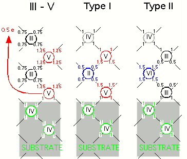
Let us begin by considering the polarity mismatch problem. The typical interface of a III-V compound on a Si(100) substrate is illustrated schematically in the left panel of the figure to the right. Each atom makes four bonds with its four neighbors. As is clear from the illustration, in order to satisfy the two-electron-per-bond counting rule, half an electron per first-layer group-V atom must be redistributed to the outer surface of the structure, thus creating a long-range electric field that accounts for the polarity mismatch.
Our solution to this problem is to reduce the valency of the second layer atoms. As is shown in the center panel of the figure, the valency of the second layer atoms is reduced by one to accommodate the extra electrons from the neighboring group-V atoms of the first layer and the third layer. In doing so, we also need to increase the valency of the fourth-layer atoms by one to satisfy the total electron counting requirement. This layering process can then be repeated without generating a long range field. Similarly, an alternative solution is to start the epitaxial layering with group-III atoms and increase or decrease the valencies of the group-V layers, as is illustrated in the right panel of the figure. In both cases, the charge-mismatch problem of the interface is resolved.
In effect, we have created a class of ``pseudo'' III-V materials, with either the group-III element replaced by a combination of group-II and group-IV elements, or the group-V element replaced by a combination of group-IV and group-VI elements. These two possibilities will be denoted as Type I and Type II materials, respectively.
It should be emphasized that there may be more than one component to
any of the three groups. For example, given group-II atoms Zn, Cd,
group-IV atoms Si, Ge, and group-V atoms P, As, one could form the
compound
...-Si-P-Zn-As-Ge-As-Cd-As-Si-...
Moreover, combinations of the two types of materials may also be
considered in epitaxial growth.
Interestingly, Type I materials have the same chemical formula as naturally-occurring Chalcopyrite materials. However, the atomic structure is different. The alternating layers of group-II and group-IV elements in Chalcopyrites are intermixed, which make layer by layer heteroepitaxial deposition difficult and also create the same polarity problem as the III-V's. The lattice structure of the Type I subclass is similar to the layered, tetragonal ABC_2 structures studied previously, where A and B are group-III elements (instead of II and IV, as in this work) and C is a group-V element.
Searching for the Right Lattice Constant
With the polarity-mismatch problem resolved, the next step is to identify candidates with lattice constants matching that of Si. Since the number of possible choices of atom types and Type I/II layered sequences is enormous, the effort to build and test the potential candidates experimentally would be formidable. In contrast, first-principle calculations on computers can go through many possibilities quickly. We proceed by searching the simple materials first and gradually increasing the complexity involved.
As a starting point, we use data on the tetrahedral-covalent radii of elements from Kittel and Shay to get the approximate lattice constants of various materials. (Detailed calculations later show that they could have an error as large as 4%.) Nonetheless, these estimated lattice constants are valuable in narrowing the search space. According to these estimates, there are 34 Type I and 41 Type II materials with lattice constants that fall within 10% of the Si lattice constant. We start by concentrating on a sampling of those within 3%, and use ab initio total energy methods to calculate more accurate lattice constants.
The total electronic energy within the local-density-approximation (LDA) is minimized using the preconditioned conjugate-gradient algorithm. The LDA calculations are performed with the Perdew-Zunger parameterized exchange-correlation energy and the Kleinman-Bylander separable form of optimized pseudopotentials. For Zn and Cd, nonlinear core corrections are used. The total energy is a function of the lattice constants as well as the basis vectors. The ions are relaxed according to the Hellman-Feynman forces for each given set of lattice vectors. The lattice constant is then located by finding the minimum of the total energy in the lattice vector space. The cutoff energy used in the calculations is E_c = 20 Ry except for materials involving first row elements, for which E_c = 40 Ry is used. The LDA method has been proven capable of predicting lattice constants to within 1% of the true values. Once materials with the correct lattice constants are found, their band structures are studied to see if they are direct band-gap materials with the desired gap size. Since LDA methods give poor band-gap results, a much more computationally intensive approach, involving the quasi-particle GW scheme, is used to obtain accurate band-gap information for the most promising candidates.
The formation enthalpies are calculated to investigate if these materials are stable against segregation into equilibrium phases of the elements. The formation enthalpies are positive, indicating the materials are stable. In the case of (ZnSi)_{1/2}As, it is 0.33 eV per atom. This is only half the value of that of the corresponding Chalcopyrite. Thus, our new material is only meta-stable. The convertion to Chalcopyrite, however, involves second-nearest-neighbor exchange and creation of interstitials. We expect the diffusion barrier to be very high and the process unlikely to occur.
A Promising Subclass
The results of the LDA study are summarized in Table (to be prepared in html). Note that the best structural candidate---(ZnSi)_{1/2}As, which has a lattice constants within 1% of that of Si, has indirect band gaps. Indeed, all of the materials listed have either indirect or marginally indirect (< 0.1 eV) gaps, except for (ZnSi)_{1/2}P and In(CS)_{1/2}. Since (ZnSi)_{1/2}P has a gap that is larger than desired and a lattice constant smaller than that of Si, it is natural to alloy it with a material that has a smaller gap and a larger lattice constant. Although there are several possible choices, we focus on one particular candidate, (ZnSi)_{1/2}As. By mixing these two materials, both the lattice constant and the band gap should be closer to the desired values. This mixing is easily done, since the epitaxial layering scheme allows us to use different group-V elements in different layers of one material. This new type of material can be written as (ZnSi)_{1/2}P_xAs_{1-x}, where x indicates the relative percentage of phosphorus used.
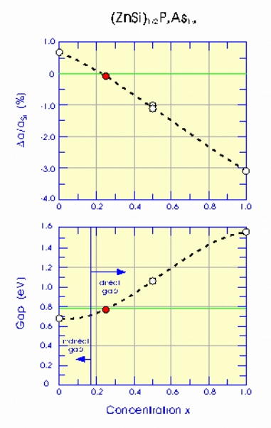
We studied several alloys with different x values, and established the
trend of lattice constant and band gap as x varies. From the figure to
the left, it is clear that a good lattice match can be found near x =
0.25, with a lattice constant only 0.08% smaller than that of Si. The
results also show that the gap is clearly direct, although marginally
so, and is about 0.78 eV. This corresponds to 1.59 µm, which
nearly matches the canonical optoelectronics wavelength. Note, the
precise value of this gap is not as important as the possibility of
tuning it by the appropriate phosphorus concentration. As it stands,
the chemical formula of this material is
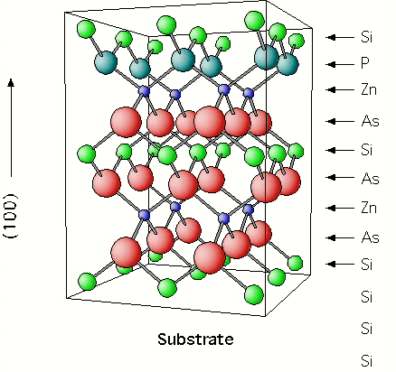
(ZnSi)_{1/2}P_{1/4}As_{3/4}. Growth of this new material on a Si(100)
substrate could then follow the sequential deposition:
As . Zn . As . Si . As . Zn . P . Si
with repetition in this order. This is shown schematically at the end.
In order to gauge how well the lattice constants continue to match as temperature increases, we can estimate the thermal expansion coefficients from the total energy surfaces for both the new material and Si. The difference in the percentage increase of the lattice constant (δa/a (T)) for the two materials is calculated to be less than 0.01% from 0K to 600K, and actually vanishes at 350K. This suggests that thermal expansion will not cause additional lattice mismatch.
Finally, the new alloy material that we have designed will possess a slight dipole moment, due to the difference in chemical properties of phosphorus and arsenic. However, this dipole moment can be eliminated if we invert every other cell in the growth direction, i.e. use a supercell twice as long in the growth direction.
We would like to thank Prof. S. Louie for his generosity in providing us with GW computer codes and Steven Johnson for helpful comments. This work was supported in part by the Office of Naval Research Contract No. N0001-94-1-0591.
References
- Ab-initio method applications
-
- A. Y. Liu and M. L. Cohen, Science 245, 841 (1989).
- A. Rubio, J. L. Corkill, and M. L. Cohen, Phys. Rev. B 49, 5081 (1994). [online]
- N. G. Chopra et al., Nature (London) 269, 966 (1995).
- A. Zunger et al., J. Electron. Mater. 22, 3 (1993).
- Z. Zunger, Int. J. Quantum Chem. Quantum Chem. Symp. 19, 629–653 (1985).
- M. L. Cohen, Philos. Trans. R. Soc. London A 334, 501–513 (1991).
- A. Zunger, Curr. Opin. Solid State Mater. Sci. 3, 32–37 (1998).
- Heteroepitaxy
-
- Heteroepitaxy in Silicon II, edited by J. Fan, J. Phillips, and B.-Y. Tsaur, MRS Symposia Proceedings No. 91 (Materials Research Society, Pittsburgh, PA, 1987).
- R. F. Davis, Proc. IEEE 79, 702 (1991).
- J. H. Edgar, J. Mater. Res. 7, 235 (1992).
- C. R. Eddy, Jr., T. D. Moustakas, and J. Scanlon, J. Appl. Phys. 73, 448 (1993).
- W. A. Harrison, E. A. Kraut, J. R. Waldrop, and R. W. Grant, Phys. Rev. B 18, 4402 (1978).
- Optoelectronics
-
- E. Desurvire, Erbium-Doped Fiber Amplifiers: Principles and Applications (Wiley, New York, 1994).
- Bond length data
-
- L. J. Shay, Ternary Chalcopyrite Semiconductors: Growth, Electronic Properties, and Applications (Pergamon, New York, 1975).
- C. Kittel, Introduction to Solid State Physics (Wiley, New York, 1996), p. 78.
- Other studies of Ternary materials
- DFT with LDA
-
- P. Hohenberg and W. Kohn, Phys. Rev. 136, B864 (1964);
W. Kohn and L. J. Sham, ibid. 140, A1133 (1965). - J. P. Perdew et al., Phys. Rev. B 23, 5048 (1981).
- D. R. Hamann, Phys. Rev. B 40, 2980 (1989); [online]
- A. M. Rappe, K. M. Rabe, E. Kaxiras, and J. D. Joannopoulos, Phys. Rev. B 41, 1227 (1990); [online]
- N. Troullier and J. L. Martins, Phys. Rev. B 43, 1993 (1991); [online]
- L. Kleinman and D. M. Bylander, Phys. Rev. Lett. 48, 1425 (1982).
- S. G. Louie, S. Froyen, and M. L. Cohen, Phys. Rev. B 26, 1738 (1982).
- M. C. Payne et al., Rev. Mod. Phys. 64, 1045 (1992).
- P. Hohenberg and W. Kohn, Phys. Rev. 136, B864 (1964);
- quasi-particle GW method