|
|
|
|
|
|
|
|
|
|
|
|
Three-Dimensional Photonic Crystals
The ideal structure to have is a three-dimensionally periodic photonic crystal (simply referred to here as a three-dimensional photonic crystal) with a full band-gap in three-dimensions. However, the complicated structure apparently required by such crystals has made them difficult to fabricate.
An Early Design
In 1994, we proposed a three-dimensional crystal designed specifically to be amenable to fabrication at sub-micron length scales. [Fan, et. al, APL 65, p. 1466-1468 (1994)] This structure, shown below, is designed to be fabricated in a layered fashion using two different dielectric materials (say, Silicon and Silicon Dioxide). Staggered channels of the lower-dielectric material pass through the high-dielectric substrate, and a triangular lattice of air holes is etched through the whole thing perpendicular to the channels.
We also have a VRML version of the primitive cell of this structure, for readers with VRML viewers. The primitive cell is duplicated (tiled) in three dimensions to form the crystal.
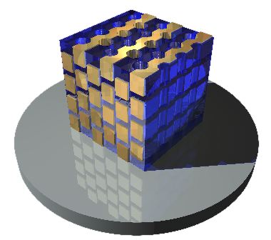
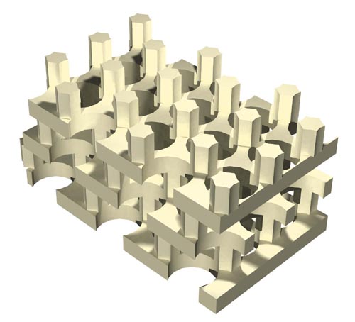
A New Layered Structure
Recently, we have proposed a new structure for achieving a full three-dimensional band gap, shown below. [S. G. Johnson and J. D. Joannopoulos, APL 77, 3490-3492 (Nov. 2000).] This structure has the unique property that its defect modes (waveguides and cavities) closely mimic those of 2d crystals. [M. L. Povinelli, Steven G. Johnson, Shanhui Fan, and J. D. Joannopoulos, PRB 64, 075313 (2001).]
This structure has three key advantages:
- It has a large, complete bandgap: over 21% for Si/air, and over 8% even for the moderate Si/SiO2 index contrast. The gap persists all the way down to 2:1 (SiO2) index ratios.
- It consists of planar layers with constant cross-sections, amenable to fabrication layer-by-layer, with a three-layer period. This allows the use of traditional lithographic techniques, along with a high degree of control in placing defects (waveguides, cavities, and other optical components) in the crystal.
- The layers themselves are an alternating stack of the two characteristic types of 2d (or slab) photonic crystals: dielectric rods in air and air holes in dielectric.
It is the third characteristic that really distinguishes this structure from previous work. The high-symmetry 2d structure of the slabs means that complicated optical networks can be constructed in this crystal by modification of only a single layer. Moreover, the types of defects and defect modes that are used to trap and guide light are strongly analogous to those in the corresponding two-dimensional or slab systems. This allows one to leverage the large body of analyses, experiments, and understanding of those simpler structures.
In other words, this structure allows you to build a "2d crystal" in 3d, but avoid the inevitable radiation losses that occur without a full 3d gap.
The fundamental structure is actually very simple: an fcc lattice (possibly distorted) of air (or low-index) cylinders in dielectric, oriented along the 111 direction. This results in the layered structure rendered above, and depicted schematically below (in vertical and horizontal cross-sections):
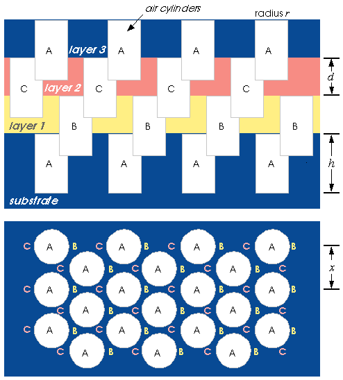
Typical parameters, for an undistorted fcc lattice of air cylinders in a dielectric constant of 12 (Si), are: d=a/sqrt(3), x=a/sqrt(2), r=0.293a, and h=0.93a, where a is the fcc lattice constant. This results in a 21% complete three-dimensional band gap, centered at a frequency of 0.569 c/a.