|
|
|
|
|
|
|
|
|
|
|
|
Waveguide Bends in Photonic Crystals
In conventional waveguides, such as fiber-optic cables, light is confined by total internal reflection (also known as index confinement, a more accurate term when the guide diameter is on the order of the wavelength). One of the weaknesses of such waveguides, however, is that creating bends is difficult. Unless the radius of the bend is large compared to the wavelength, much of the light will be lost. This is a serious problem in creating integrated optical "circuits," since the space required for large-radius bends is unavailable.
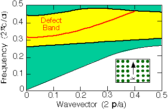
Photonic crystal waveguides operate on a different principle. A linear defect is created in the crystal which supports a mode that is in the band gap. This mode is forbidden from propagating in the bulk crystal because of the band gap. (That is, waveguides operate in a manner similar to resonant cavities, except that they are line defects rather than point defects.) Below, we see the dispersion relation for the guided mode created in a 2d photonic crystal (square lattice of rods) by removing a row of rods:
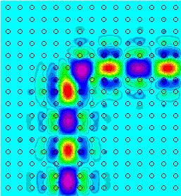
When a bend is created in the waveguide, it is impossible for light to escape (since it cannot propagate in the bulk crystal). The only possible problem is that of reflection. However, the problem can be analyzed in a manner similar to one-dimensional resonant tunneling in quantum mechanics, and it turns out to be possible to get 100% transmission. The following picture depicts the electric field in a waveguide bend exhibiting 100% transmission.