Results
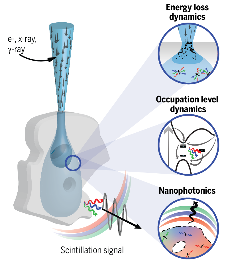
Figure 1 (left): A general framework for scintillation in nanophotonics. Nanophotonic scintillators consist of nanophotonic structures integrated in scintillators. We develop a framework to model, tailor, and optimize scintillation by combining energy loss dynamics, occupation level dynamics, and nanophotonics modeling.
Theory. First, we present a unified theory of nanophotonic scintillators. The theory we develop is ab initio : it can, from first principles, predict the angle- and frequency-dependent scintillation from arbitrary scintillators integrated with nanostructures, taking into account the three steps illustrated in Figure 1. It takes into account the energy loss dynamics of high-energy particles through arbitrary materials, the non-equilibrium steady state and electronic structure of the scintillating electrons, and the nanostructured optical environment (i.e., the electrodynamics of the light emission by this non-equilibrium electron distribution). One central result of our work is the use of electromagnetic reciprocity to efficiently calculate scintillation in nanophotonics. Reciprocity connects far-field scintillation calculation to the computation of absorption "maps" from plane waves. Using the theory as a guide, we demonstrated order-of-magnitude scintillation enhancements in two different platforms: electron-induced scintillation by silica defects, and x-ray induced scintillation by rare-earth dopants in conventional scintillators. The enhancements in both cases were enabled by two-dimensionally-periodic etching either of the scintillator or the material above the scintillator to create a two-dimensional photonic crystal.
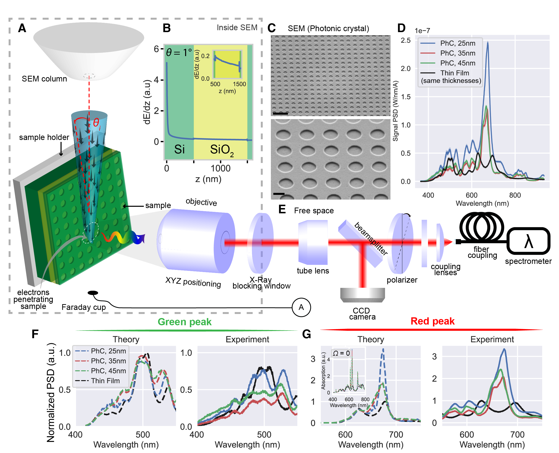
Figure 2 (above): Experimental demonstration of nanophotonic shaping and enhancement of electron-beam-induced scintillation. (A) A modified scanning electron microscope (SEM) is used to induce and measure scintillation from electron beams (10 - 40 keV) bombarding scintillating nanophotonic structures. (B) Electron energy loss in the silicon-on-insulator wafer is calculated via Monte Carlo simulations. Inset: Zoomed-in electron energy loss in the scintillating (silica) layer. (C) SEM images of photonic crystal (PhC) sample (etch depth 35 nm). Tilt angle 45°. Scale bar: 1 μm (top), 200 nm (bottom). (D) Scintillation spectrum from thin film (TF) and PhC samples with varying etch depths (but same thickness). (E) The scintillation signal is coupled out of the vacuum chamber with an objective and then imaged on a camera and analyzed with a spectrometer. (F-G) Comparison between theoretical (left) and experimental (right) scintillation spectra for green and red scintillation peaks. Inset: Calculated scintillation spectra (per solid angle) at normal emission direction, showing the possibility of much larger enhancements over a single angle of emission.
Electron-beam experiments. In a first set of experiments, we measured nanophotonic-enhanced scintillation from silica defects in a silicon-on-insulator platform. We compared the scintillation from several samples, including a thin film (TF) sample (of silicon atop silica atop silicon) and a photonic crystal (PhC) sample, from the same wafer but patterned with a two-dimensional periodic lattice of holes. The scintillation spectra of the samples in the visible range are shown in Figure 2D. The multiple peaks of the spectra are well accounted for at both red and green wavelengths by our theory. The bulk spectrum is inferred from previous observations and confirmed by our density functional theory calculations. In contrast to the TF scintillation, the scintillation from the PhC samples displays very strong and spectrally-selective enhancement. We report an enhancement of the red scintillation peak in the PhC sample, compared to the TF, by a factor of ~6 (peak at 674 nm) and of ~3 integrated over the main red peak (665 ± 30 nm) as shown in Figure 2D. This feature is reproduced by our theoretical framework around the red scintillation peak, using the same fitting parameters as those taken from the TF results of Figure 2F-G. The observed enhancement can readily be attributed theoretically to the presence of high-Q (quality factor) resonances at the red wavelength, which lead to enhanced absorption of light in the far-field. More information about the experimental setup can be found in previous references from our group [see for instance Kaminer et al. PRX (2017); Yang et al. Nature Physics (2018); Roques-Carmes et al. Nature Communications (2019)].
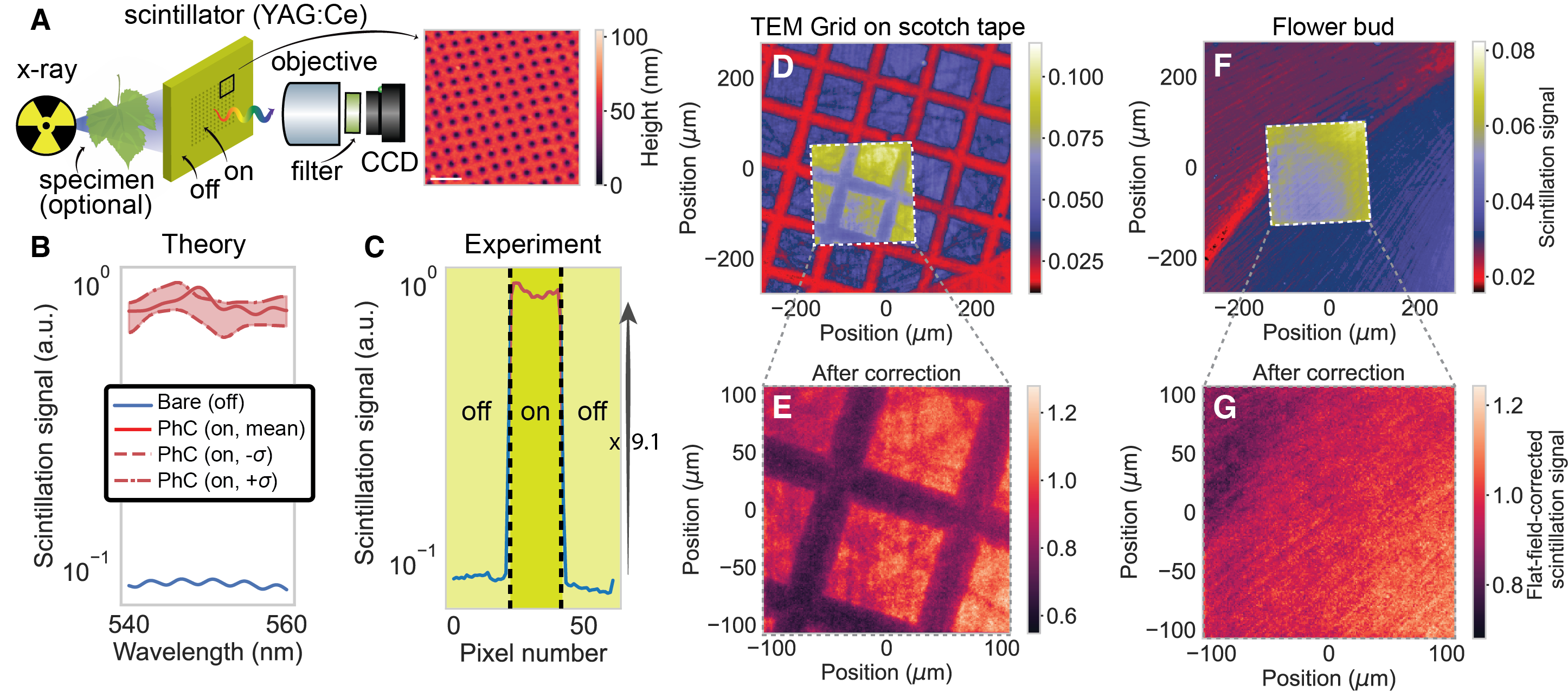
Figure 3 (above): X-ray scintillation enhancement and imaging with nanophotonic scintillators. (A, Left) X-ray scintillation experimental setup: light generated by x-ray bombardment of a cerium-doped yttrium aluminium garnet (YAG:Ce) scintillator is imaged with a set of free-space optics. A specimen may be positioned between the source and the scintillator to record an x-ray scan of the specimen. (A, Right) Atomic force microscopy image of patterned YAG:Ce scintillator (20 μm thickness). Scale bar: 1 μm. (B) Calculated scintillation spectrum of the PhC, integrated over the experimental angular aperture. (C) Measured scintillation along a line of the sample, including regions on (red) and off (blue) the PhC. The scintillation from the PhC region is on average about x9.1 higher than the unpatterned region. (D, F) Measured x-ray images of a (D) TEM grid on scotch tape and of a (F) flower bud. The white square delimits the PhC area. (E, G) Flat-field corrected zoom-in of the x-ray image in the PhC area. Compared to the unpatterned regions, the images are brighter above the PhC region, and show no evident decrease in resolution. The particular nanophotonic scintillator used for this experiment was patterned over an area of 430 μm x 430 μm and resulted in a scintillation enhancement of x2.3 (measured with respect to unpatterned scintillator of same thickness).
X-ray experiments. In a second set of experiment, we recorded scintillation enhancement from nanopatterned x-ray scintillators [cerium-doped yttrium aluminium garnet (YAG:Ce)]. We also used these nanophotonic scintillators to record x-ray images in a micro-CT scanner and observed subsequent image brightness enhancements. The results are shown in Figure 3. We used the typical x-ray imaging configuration shown in Figure 3A: x-rays traverse a specimen, leading to spatially-dependent absorption of the incident x-ray flux. This absorption pattern is geometrically magnified until it encounters the YAG:Ce scintillator. This absorption pattern is then translated into scintillation photons which are imaged with an objective and a CCD camera. The nanopatterned scintillator is constructed by etching a two-dimensional PhC into YAG:Ce [via Focused Ion Beam (FIB) lithography], at the surface of the scintillator facing the objective.
According to the scintillation framework developed in our paper, nanophotonic scintillation enhancement is to be expected when the absorption of light is enhanced. Here, the calculated enhancement is by a factor of ~9.3 over the measured scintillation spectrum. The x-ray scintillation enhancement originates in light out-coupling enhancement (or by reciprocity, in-coupling enhancement). This effect is of the type often leveraged to design more efficient LEDs and solar cells that approach the "Yablonovitch limit" in both ray-optical, and nanophotonic settings. Our theory matches well our experimental measurements. The experimentally measured scintillation scanned along a line of the sample is shown in Figure 3C. The signal is enhanced on average by a factor of ~9.1 over the unpatterned region. To demonstrate the potential of our approach to x-ray imaging, we fabricated a larger-scale pattern on a 50 μm wafer which exhibits a scintillation enhancement of x2.3. We recorded single-shot x-ray scans of biological and inorganic specimens through the PhC, showing no evident decrease in resolution, while increasing the image brightness by the same factor. Equivalently, the required x-ray dose or exposure time to get a given number of counts on the detector is reduced.