Background & Motivation: Method:Computers that can learn, combine, and analyze vast amounts of information quickly, efficiently, and without the need for explicit instructions are a powerful tool for handling large datasets. "Deep learning" algorithms have received an explosion of interest in both academia and industry for their utility in image recognition, language translation, decision-making problems, and more. Traditional central processing units (CPUs) are suboptimal for implementing these algorithms, and a growing effort in academia and industry has been put towards the development of new hardware architectures tailored towards applications in artificial neural networks and deep learning. Graphical Processing Unit (GPUs), Application Specific Integrated Circuits (ASICs) and field-programmable gate arrays (FPGAs), including IBM TrueNorth and Google TPU, have improved both energy efficiency and speed enhancements for learning tasks. In parallel, hybrid optical-electronic systems that implement spike processing and reservoir computing have been shown. In
this project, we explore mostly- and fully-optical architecture for
implementing general deep neural network algorithms using nanophotonic
circuits that process coherent light. The speed and power efficiency of
our proposed architecture are largely enabled by coherent, fully-optical
matrix multiplication (a cornerstone of neural network algorithms).
Under the assumption of practical, centimeter-scale silicon photonic die
sizes and low waveguide losses, we estimate that such an optical neural
network would enable forward-propagation at
least two orders of magnitude faster than state-of-the-art electronic
or hybrid optical-electronic systems and with a power consumption that
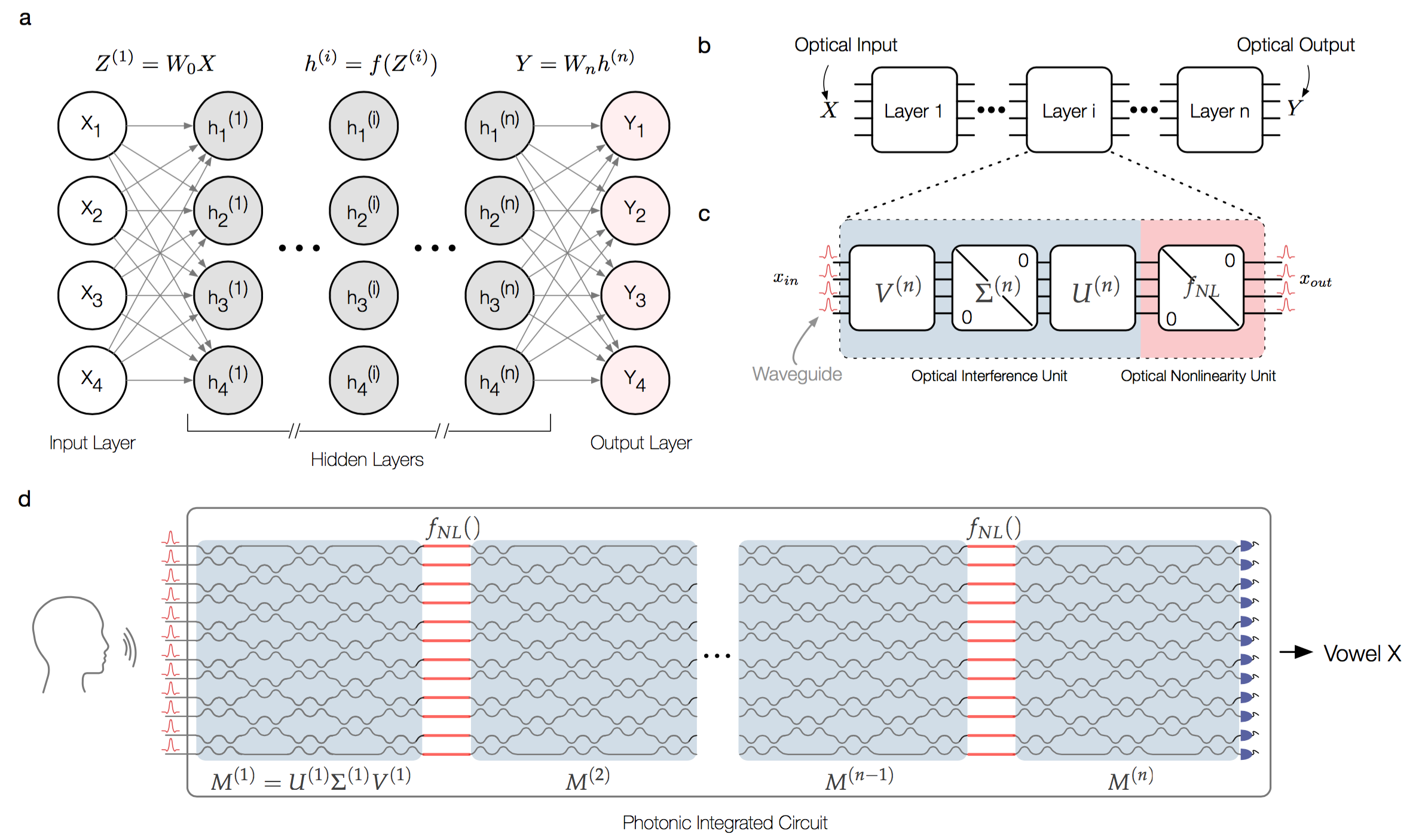
is nearly proportional (instead of quadratic as in electronics) to the number of neurons. FIG. 1. General Architecture of Optical Neural Network a. General artificial neural network architecture composed of an input layer, a number of hidden layers, and an output layer. b. Decomposition of the general neural network into individual layers. c. Optical interference and nonlinearity units that compose each layer of the artificial neural network. d. Proposal for an all-optical, fully-integrated neural network. Experimental setup and observation.
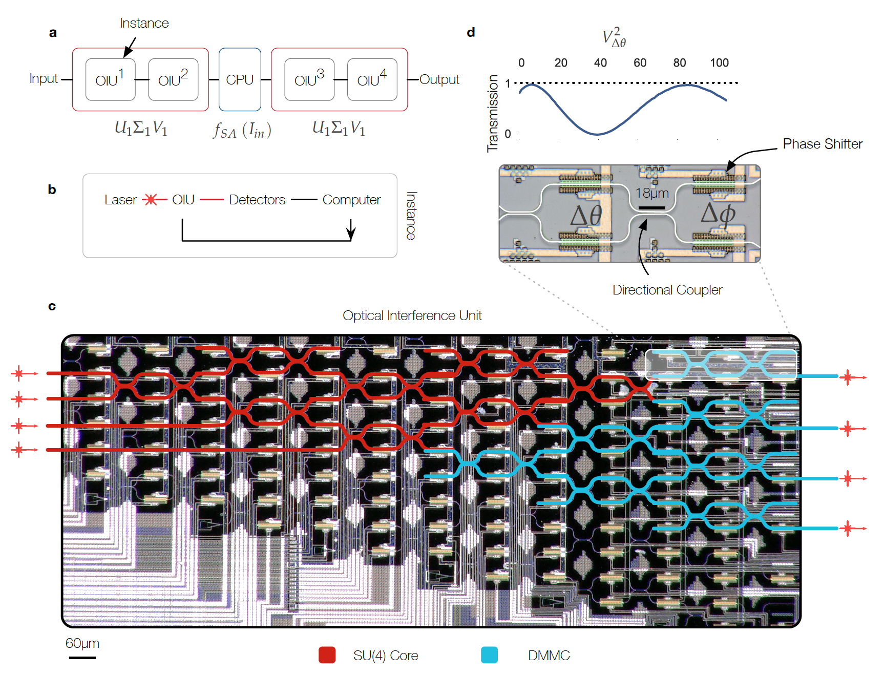
In a proof of concept experiment, we implement the optical interference unit (OIU) using the programmable nanophotonic processor (PNP). The PNP is a silicon photonic integrated circuit fabricated in the OPSIS foundry. It is composed of 56 programmable Mach-Zehnder Interferometers (MZIs). Programmable MZIs are composed of a thermo-optic phase shifter (θ) between two 50% evanescent directional couplers and followed by another phase shifter (φ). The MZI splitting ratio is controlled with the internal phase shifter (as shown in Fig. 2(d)) and the differential output phase is controlled with the external phase shifter. As shown in Fig. 2(a,b), we re-program the PNP to realize all of the required OIUs, and simulate the nonlinear transfer function of a saturable absorber (see Eqn 1) on a computer. This proof-of-concept demonstration requires photodetection and re-injection of light into the PNP modes between layers of the neural network. However, given the compactness of the required section of the PNP, all five layers of the PNP could be integrated on a chip less than a centimeter in length. FIG. 2. Illustration of Optical Interference Unit a. Schematic representation of our 2-layer ONN experiment. The programmable nanophotonic processor is used 4 times to implement the deep neural network protocol. After the first matrix is implemented, a nonlinearity associated with a saturable absorber is simulated in response to the output of layer 1. b. The experimental feedback and control loop used in the experiment. Laser light is coupled to the OIU, transformed, measured on a photodiode array, and then read on a computer. c. Optical micrograph illustration of the experimentally demonstrated optical interference unit which realizes both matrix multiplication (highlighted in red) and attenuation (highlighted in blue) fully optically. The spatial layout of MZIs follows the Reck proposal enabling arbitrary SU(4) rotations by programming the internal and external phase shifters of each MZI (θi , φi ). d. Schematic illustration of a single phase shifter in the Mach-Zehnder Interferometer and the transmission curve for tuning the internal phase shifter. After
programming the nanophotonic processor to implement our ONN
architecture, which consists of 4 layers of OIUs with 4 neurons in each
layer (which requires training a total of 4 · 6 · 2 = 48 phase
shifter settings), we evaluated it on the vowel recognition test set.
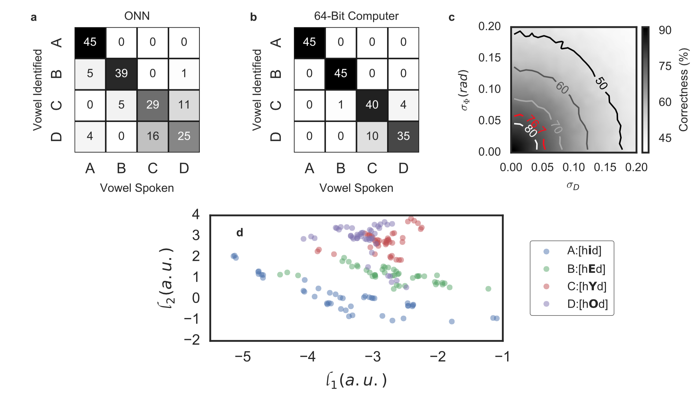
Our ONN correctly identified 138/180 cases (76.7%) compared to the
correctness of 165/180 (91.7%) computed with a conventional 64-bit
digital computer. The difference between the ONN and the digital
computed results is mainly caused by the difference in their
computational resolution. As can be seen from Fig. 3(a,b),
both systems are good at classifying vowel A and vowel B; while for
vowel C and vowel D even the 64-bit computer is having some difficulties
in classifying them, showing that these two vowels are relatively close
in the parameter space we used (Fig. 3(d)). As a result, our ONN have even more misclassification on these two vowels due to its limit in resolution. FIG. 3. Vowel recognition. (a-b) Correlation matrices for the ONN and a 64-bit electronic computer, respectively, implementing 2-layer neural networks for vowel recognition. Each row of the correlation matrices is a histogram of the number of times the ONN or 64-bit computer identified vowel X when presented with vowel Y. Perfect performance for the vowel recognition task would result in a diagonal correlation matrix. (c) Correct identification ratio in percent for the vowel recognition problem with phase encoding (σΦ) and photo-detection error (σD); the definition of these two variables can be found in method section. Solid lines are contours for different correctness ratios. In our experiment, σD ≃ 0.1%. The contour line shown in red marks an isoline corresponding to the correct identification ratio of our experiment. (d) Two-dimensional projection (log area ratio coefficient 1 on the x-axis and 2 on the y-axis) of the testing dataset which shows the large overlap between spoken vowel C and D. This large overlap leads to lower classification accuracy for both a 64-bit computer and the experimental ONN. References: More detailed description of this work can be found in our paper published in Nature Photonics, June 12th, 2017:
3 decades ago, there was also a lot of interest in optical NNs. For a good review, please see:
We believe that some of these ideas are definitely worth revisiting now that neural networks are of such a huge importance in the AI community, and now that the integrated optics matured to the point where optical neural networks could potentially be produced in a truly manufacturable way. Some nice news article was written about this work: In English:
New system allows optical “deep learning", by David Chandler (MIT News) Light-Powered Computers Brighten AI’s Future, by Jesse Dunietz (Scientific American) Computer chip mimics human brain, with light beams for neurons, by Matthew Hutson (Science)Deep Learning at the Speed of Light on Nanophotonic Chips, by Edd Gent (SingularityHub)MIT研发光学深度神经网络:几乎不需能耗, by 安妮 (搜狐新闻)Press Coverages also includes: In English In Chinese In Other Languages Spektrum (Germany), Entrelineas (Spanish) Commercialization: We have also spent some time thinking about commercializing this technology, some press release related to this includes: Winning Harvard President Innovation Challenge (2017) (Harvard Gazette) |


